
May 25, 2026, 7:38 a.m. ET | ⏱️6–7minutes
By Olivia Bennett
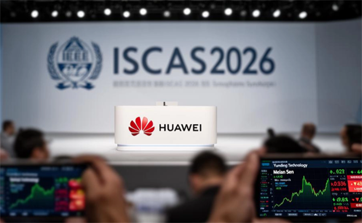
On May 25, 2026, at the IEEE International Symposium on Circuits and Systems (ISCAS 2026), Huawei Board Member and Semiconductor Business President He Tingbo delivered a keynote titled “Exploration and Practice of a New Path for Semiconductors.” She also released a preprint paper on ChinaXiv introducing a new framework called the “Tao (τ) Law.”
The central idea is straightforward: instead of measuring semiconductor progress mainly by how small transistors become, the industry should increasingly focus on reducing overall system-level signal latency.
This article reviews the key claims, industry reactions, and unresolved questions surrounding the proposal.
Why the Industry Is Searching for New Directions
Since Gordon Moore’s 1965 prediction that transistor counts on integrated circuits would double regularly, semiconductor progress has largely depended on geometric scaling.
But the two major foundations behind this model have weakened over time.
The first issue is the breakdown of Dennard scaling.
For decades, shrinking transistors also reduced voltage and power consumption proportionally. Around 2005–2007, however, this relationship began to fail. Voltage scaling slowed, power density increased, and boosting chip frequencies became far more difficult.
Multiple industry and academic sources have described this turning point, including SemiEngineering, IEDM coverage, and educational analyses discussing post-2005 power-density challenges.
The second issue is economics.
Industry estimates from IBS suggest that designing a 28nm chip once cost roughly $51 million. By 7nm, estimates had risen to around $300 million. For 3nm and 2nm nodes, various reports place development costs between roughly $500 million and over $1 billion, depending on complexity and tape-out requirements.
While figures vary across reports, the broader trend is widely recognized: transistor scaling is becoming dramatically more expensive.
Against this backdrop, He Tingbo’s team argued in their paper that the industry’s central question is no longer:
“How much smaller can we make the transistor?”
Instead, the focus may increasingly become:
“What exactly should be scaled, and toward what goal?”
The Core Idea of the “Tao Law”
At the center of the framework is a time constant called “τ” (tau).
According to Huawei’s proposal, τ measures the total delay between issuing a signal and completing a full system-level response.
In practical terms, traditional semiconductor scaling focused heavily on space:
· How many transistors fit into a chip area?
· How dense can the layout become?
The Tao framework instead emphasizes time:
· How quickly can the entire system complete a task?
· How much delay exists across the full computing path?
He Tingbo wrote that future electronic-system evolution “should be guided not by geometric scaling but by temporal scaling.”
Importantly, Huawei does not present this framework as a rejection of advanced manufacturing nodes. Instead, the proposal reframes cutting-edge lithography as one possible optimization path rather than the only path.
Whether the wider industry will ultimately recognize this framework as a new “law” remains uncertain.
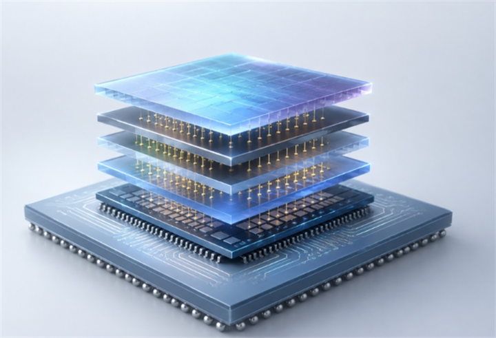
“LogicFolding” and Huawei’s Engineering Claims
To implement τ-based scaling, Huawei introduced a design methodology called “LogicFolding.”
According to public descriptions, the approach vertically stacks digital, analog, and memory circuits into active layers. The goal is to shorten critical signal paths and reduce RC delay caused by resistance and capacitance.
At ISCAS 2026, He Tingbo stated that the planned “Kirin 2026” chip would become the first full engineering implementation of the method.
Huawei’s presentation slides showed several projected gains:
· Estimated transistor density increasing from roughly 155 MTr/mm² to 238 MTr/mm²
· About 41% improvement in performance-core energy efficiency
· Peak frequency rising approximately 12.7% to 3.1 GHz
These figures were later cited by multiple technology outlets.
However, several caveats are important.
First, the baseline density figure of 155 MTr/mm² was itself labeled an estimate in some reporting.
Second, all results currently originate from Huawei’s own disclosures. No independent third-party verification has yet been published.
He also stated that Huawei had mass-produced 381 chip designs between 2020 and 2026 across mobile, AI, automotive, and infrastructure markets. Multiple Chinese media outlets repeated this figure, though it likewise remains company-disclosed information.
Industry Reactions: Interest and Skepticism
The Tao Law has generated both enthusiasm and criticism.
Some academics see value in the framework.
Professor Zhou Jianjun of Shanghai Jiao Tong University reportedly suggested that the proposal offers semiconductor firms an alternative route when access to advanced manufacturing equipment becomes constrained. From this perspective, architectural innovation and system-level optimization could partially compensate for process limitations.
At the same time, skeptics argue that many of the ideas resemble existing concepts already discussed within the semiconductor industry.
Several analysts noted similarities to “System Technology Co-Optimization” (STCO), an industry direction previously promoted by organizations such as IMEC, Intel, and TSMC. STCO has been discussed in the International Roadmap for Devices and Systems (IRDS) for years, especially alongside advanced packaging and 3D integration.
Some commentators on Chinese tech forums argued that the Tao framework may function more as a systematic summary of existing engineering approaches than as an entirely new scientific law.
Other observers focused on practical concerns.
Questions remain about:
· Thermal management
· Manufacturing yield
· Stacking-related costs
· Access to advanced EDA tools
· Long-term scalability
Several media outlets also emphasized that both excessive praise and outright dismissal may be premature.
At this stage, the concept remains under active debate.
Huawei’s Long-Term Roadmap
According to Huawei’s ISCAS 2026 roadmap slides, the company hopes that by 2031 its approach could achieve:
· Performance comparable to a 1.4nm-class node
· More than 400 MTr/mm² transistor density
· Clock frequencies reaching 5.0 GHz
These figures are future targets rather than demonstrated achievements.
Major engineering challenges still remain unresolved, including heat dissipation, manufacturing economics, software-tool coordination, and production yield.
Whether such goals can ultimately be reached is still unknown.
Another interesting detail is that He Tingbo released the full paper through ChinaXiv rather than the more internationally familiar arXiv platform.
Some observers interpreted this as part of a broader diversification in scientific publishing channels. However, that interpretation remains speculative rather than definitive.
Conclusion
The “Tao Law” can be viewed as Huawei’s attempt to rethink semiconductor progress during a period of growing physical, economic, and geopolitical constraints.
Rather than focusing exclusively on transistor miniaturization, the framework shifts attention toward reducing overall system latency and improving architectural efficiency.
Supporters see it as a potentially useful engineering direction under increasingly difficult scaling conditions.
Critics argue that many underlying ideas already exist within established STCO and advanced-packaging discussions.
At present, the framework remains an early-stage proposal that still requires broader validation, independent verification, and long-term industry testing.
For now, cautious observation may be more valuable than quick conclusions.
References
[1] Moore, G. E. (1965). Cramming More Components onto Integrated Circuits. Electronics, 38(8), 114–117.
[2] Dennard, R. H., Gaensslen, F. H., Rideout, V. L., Bassous, E., & LeBlanc, A. R. (1974). Design of Ion-Implanted MOSFET’s with Very Small Physical Dimensions. IEEE Journal of Solid-State Circuits, 9(5), 256–268.
[3] International Business Strategies (IBS). (2024). Semiconductor Design Cost Trends.
[4] International Roadmap for Devices and Systems (IRDS). (2022). System Technology Co-Optimization White Paper.
[5] He, T. (2026). A New Path for Semiconductors: Exploration and Practice. ChinaXiv preprint, No. 202605.00224.
About the Author
Olivia Bennett specializes in emerging technologies, including artificial intelligence, robotics, space technology, and biotechnology. Drawing on industry research and public data, she explores the technological, commercial, and societal implications of major innovations, with an emphasis on balanced and accessible analysis.
Editor’s note:
This article summarizes publicly available information and industry commentary regarding Huawei’s proposed “Tao Law” framework presented at ISCAS 2026. Some technical figures, roadmap targets, and performance claims originate from Huawei and have not yet undergone independent third-party verification. The discussion remains ongoing, and readers are encouraged to view current claims with appropriate caution.
Recommend:

Which of Space, Brain-Computer, or Genetics Might Blend into Daily Life First?

Huawei’s “Tao Law” Could Reshape How Future Chips Are Designed
Perovskite Solar Cells: High Efficiency, but Can They Last?

Why Precision Feeding with Cattle Facial Recognition Is Stalling